At MCH I met up with a few maps people and worked on a GPS app for the badge. After that I decided I should make my own add-on with a GPS antenna, and that I wanted to design and print the antenna on a PCB. I succeeded, and here is the story.
Analysis
I consulted several books and papers. A regular patch antenna is a pretty common and simple thing, but GPS is a circularly polarized signal, and that part is a bit more obscure.
- Antenna Theory: Analysis and Design
- Microstrip Antenna Design Handbook
- Circularly Polarized Antennas
To start simple I decided to make a regular patch antenna first and then try to modify it for circular polarization. So I took some equations from the Belanis book and arrived at the following code to calculate the dimensions for a rectangular patch antenna for the L1 GPS frequency of 1574MHz:
from scipy.constants import c, mu_0, epsilon_0
import math

f0 = 1574e6
eps_r = 4.5
h = 1.6e-3

# CP uses this as initial guess for L too
W = c/(2*f0)*math.sqrt(2/(eps_r+1))
print("W:", W*1e3, "mm")

eps_eff = (eps_r+1)/2 + (eps_r-1)/2*(1+12*h/W)**-0.5
print("eps_eff:", eps_eff)

DL=h*0.142*((eps_eff+0.3)*(W/h+0.264))/((eps_eff-0.258)*(W/h+0.8))
print("DL:", DL*1e3, "mm")

L = 1/(2*f0*math.sqrt(eps_eff*mu_0*epsilon_0))-2*DL
print("L:", L*1e3, "mm")
That it pretty much the extent of analysis I did. For the feedline I used the KiCAD PCB calculator to calculate the width of a 50Ω transmission line. To fine-tune everything I just did a lot of parameter sweeps in the simulator.
As far as designing the CP antenna goes, none of the books IMO strike a good balance of giving useful and understandable theory about CP. They kind of hand-wave about disturbances and throw some integrals at you. So in the end I just went with the truncated corner design and did some sweeps on how much to chop off.
Simulation
At first I tried to simulate the antenna with OpenEMS, based on modifying their simple patch antenna tutorial. But I got really weird results and kind of gave up on that idea. I had seen Andrew Zonenberg do a lot of EM simulations in Sonnet, and they were kind enough to provide me with a trial license for this project, as well as amazing support. I really can’t recommend them enough. As Andrew says: OpenEMS might be good in the future, but right now if you value your time, Sonnet is the way to go.
My analysis suggested a patch size of around 45mm, so I tried to set up a sweep in Sonnet, but was having issues where different widths would give exactly the same results. I’m just going to quote the entire email I received from their support, who are total experts in their domain:
The reason why you are observing stepped behavior in your parameter sweep responses is because the variable step is smaller than the cell size and the metal is off grid. The variable L is swept from 44 to 46 mm, with a step of 0.1 mm:
The cell size is 1.27 x 1.27 mm:
Below is a screenshot of the geometry with the dimension parameters displayed:
The Sonnet EM solver analyzes the metal as it is snapped to the grid. This means the following:
- When L is 44 mm, the metal snapped to the grid is 44.45 mm (35 cells).
- When L is 45 mm, the metal snapped to the grid is 44.45 mm (35 cells).
- When L is 46 mm, the metal snapped to the grid is 45.72 mm (36 cells).
The dependent parameter Y equals L/7.5 mm.
- When L is 44 mm, Y = 5.866 mm. The snapped dimension would be 6.35 mm (5 cells).
- When L is 45 mm, Y = 6.0 mm. The snapped dimension would be 6.35 mm (5 cells).
- When L is 46 mm, Y = 6.133 mm. The snapped dimension would be 6.35 mm (5 cells).
With the specified parameter sweep of L of 44 to 46 mm, step of 0.1 mm, effectively the L dimension is 6.35 mm in all combinations. The key then is to work with a smaller cell size, to resolve the small dimensional changes. A smaller cell size will increase the memory requirement and analysis time, so there is a tradeoff. In the attached “feedviapatch_gk” model variation, I made a number of modifications:
- Cell Size – Reduced cell size from 1.27 x 1.27 mm to 0.2 x 0.2 mm. This will resolve smaller dimension changes and match the patch dimensions better, which are whole numbers 45 x 45 mm
- Via Port- The via size for the Via Port was 1.27 x 1.27 mm. I snapped this via to the new grid, reducing it to 1.2 x 1.2 mm. This should have minimal impact on the response.
- Box Size - Wavelength with Er=1, at 1.575 GHz is 190 mm. For antenna models, we recommend approximately 2 wavelengths or more clear area around the antenna. Specified a box size of 800 x 800 um, which is a reasonable size. With a relatively large box size and relatively small cell size, this will lead to a large number of cells. In this model it is 4000 x 4000 number of cells, which is reasonable. As the number of cells reaches 20000 or more, the analysis time will increase substantially.
- Upper air layer thickness – With an antenna model, with the box bottom cover used as a lower groundplane, the upper air layer thickness should be approximately 0.5 wavelength. Specified a value of 95 mm.
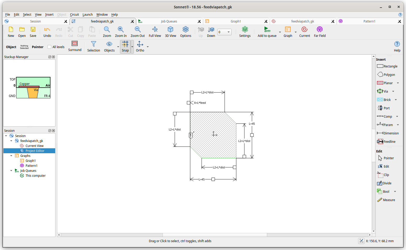
- Patch position and orientation – Centered the patch and rotated it 90 degrees clockwise
- Symmetry – Enabled symmetry. With the centered patch and new orientation, symmetry can be used to substantially reduce the memory requirement and analysis time.
- Via Port position variable – Deleted the existing X and Y dimension parameters. Redefined a new X parameter. A new Y dimension parameter was not required as the Via Port remains centered.
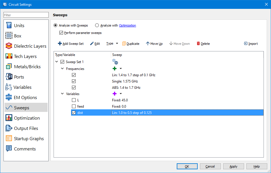
- Parameter sweep - Changed parameter sweep of L to 44 to 46 um, step 1 mm. All of the L values will be resolved and fall on the grid. The X values will be 5.866, 6, and 6.133 mm. Due to the 0.2 x 0.2 mm grid, these will be snapped to 5.8, 6, and 6.2 mm.
Below is a dB[S11] plot comparing the response at L values of 44, 45, and 46 mm:
For finer resolution, you could use a 0.1 x 0.1 mm cell size, but this will come at the expense of additional memory and analysis time. The change in the X variable value will drive the cell size. For example a 1 mm change in L, results in a 1/7.5 = 0.133 mm change in X.
For this model, the total analysis time on my desktop machine was 5 minutes, 37 seconds. The reported memory requirement was only 2 MB, because the Lite EM solver only counts one portion of the analysis. You can see the actual memory requirement in the logfile, which was 146 MB.
The attached model is a packed project archive (zon extension) with data. You can open it as you would a project file (son extension). Since it already includes data, you do not need to reanalyze and can plot the S-parameter and current density data.
Wow I did a learn. Amazing. After that I could easily run some sweeps and find an antenna size suitable for GPS reception. From here things happened kind of in parallel, but for the sake of the story let’s move on to simulating the CP antenna.
I had two more minor problems with this antenna. First is that it’s no longer symmetrical so I should turn off that setting again. The other is that circular polarization requires far-field analysis, and far-field analysis requires a full EM solve at the desired frequency. When you just do a normal sweep Sonnet tries to be smart and interpolate a bunch of things, so if you want to compare data from different parameters, you actually need to tell it to do a full EM solve at that frequency by adding a linear sweep and/or a single frequency.
Then you can set up and parameterize a truncated patch and do some sweeps:
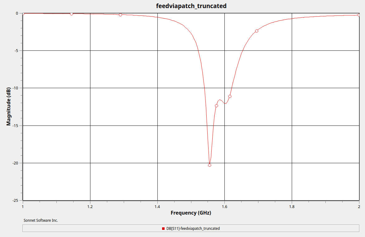
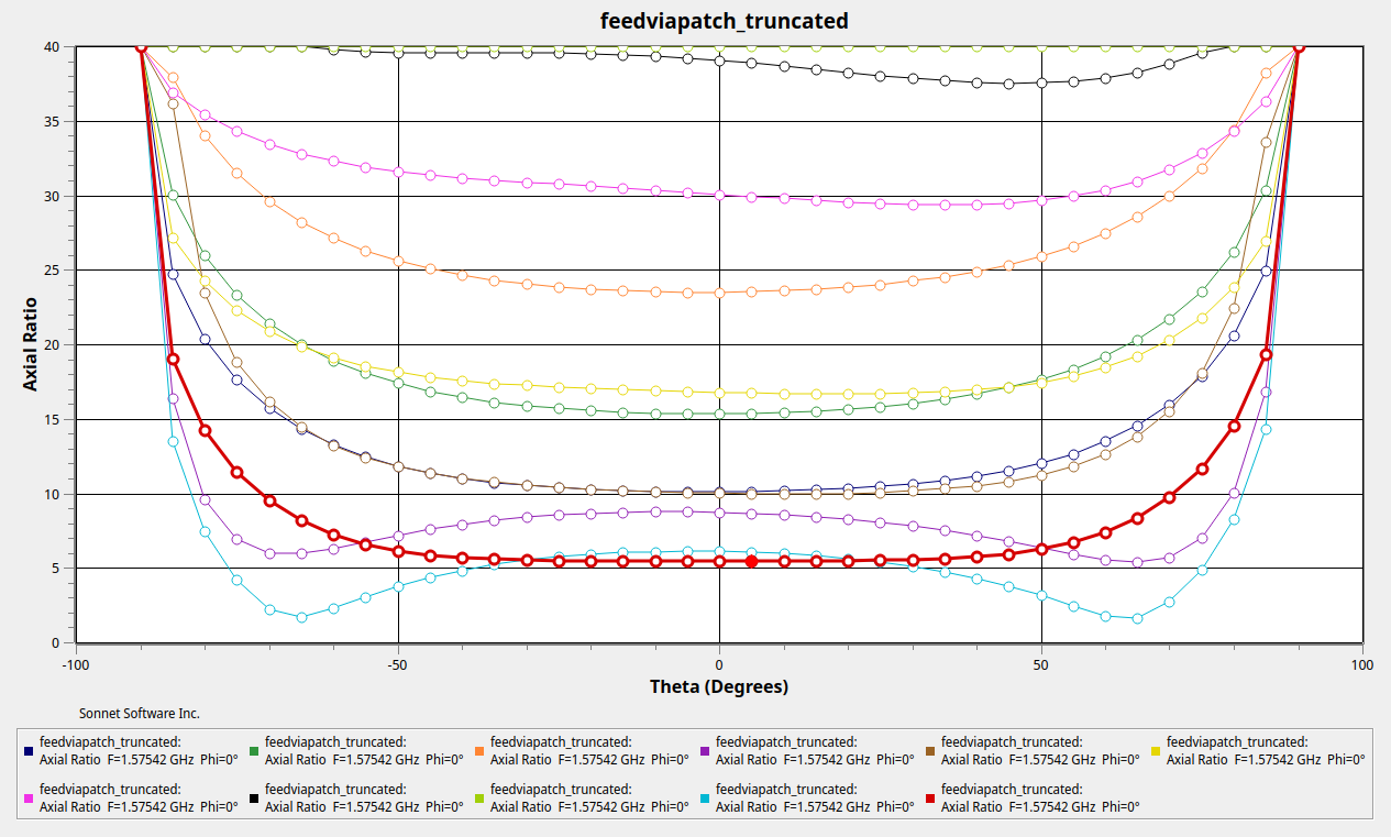
Here is the S11 of my final antenna and some sweeps of the axial ratio of the far field.
Construction
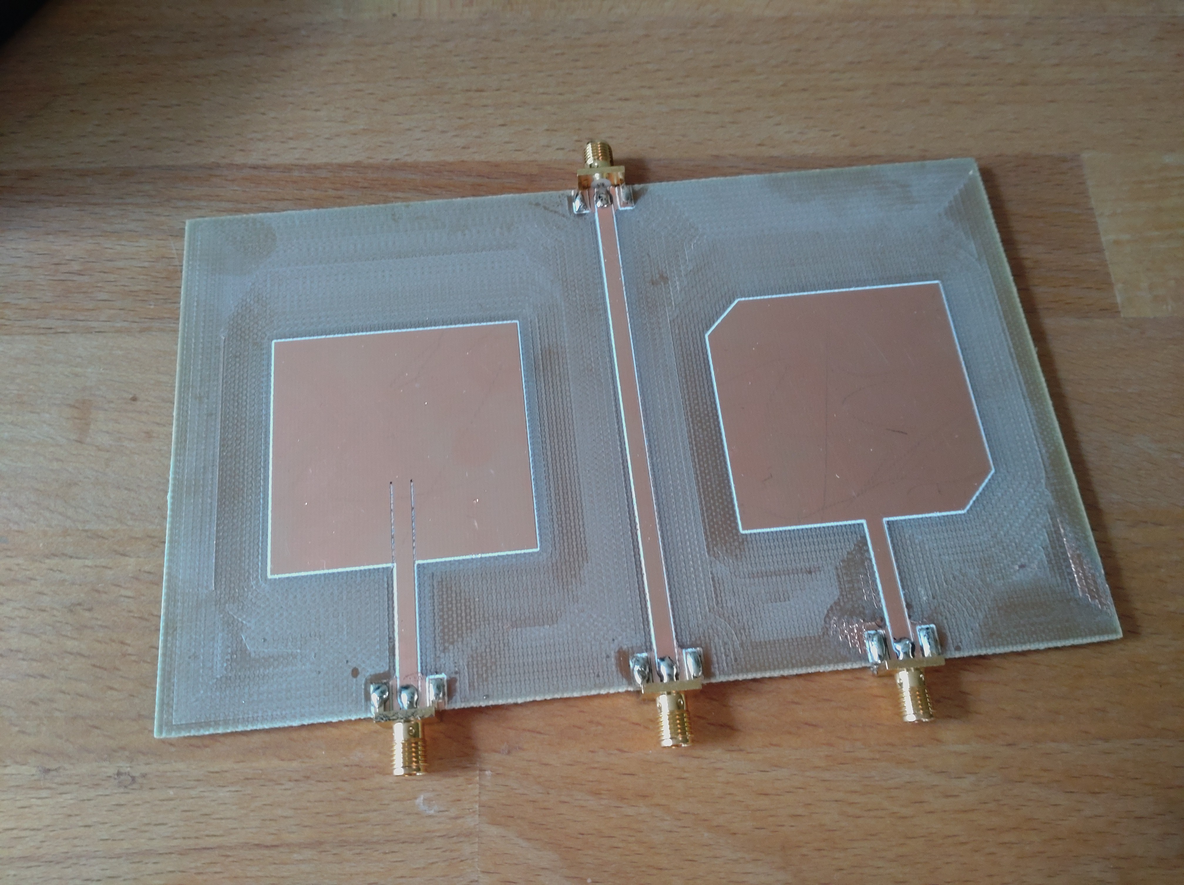
After the simulations it was finally time to make some antennas. I decided the best way to prototype these things was to use the CNC at Tkkrlab to mill a double sided PCB blank into an antenna and solder some SMA connectors to it. First I drew the antenna in KiCAD using SMD pads as the patch, there is even an option to make chamfered pads. I also added a stripline to callibrate the width.

Then I exported the PCB design to Gerber, loaded it into FlatCAM to convert it to a toolpath, and used bCNC to execute it. The process is a bit unintuitive and requires some experimentation, but nothing too crazy. I was able to just show up to Tkkrlab with my gerber files, create toolpaths, put on PPE, and watch my antenna being made. I used a 3mm flat bit to clear all the metal, and then a pointy bit to route the edges for exact dimensions and to get the SMA pads cut.
Measurement
For testing the impedance of the antenna as well as the S11 I got myselve a LiteVNA. For the rectangular patch, I cut slots at the feedline to reduce the impedance, and for the truncated patch I was worried I’d have to construct some RF magic like a quarter wave transformer or hybrid but for some reason the impedance was actually kinda alright. Here is what the readout of the truncated andenna looks like:
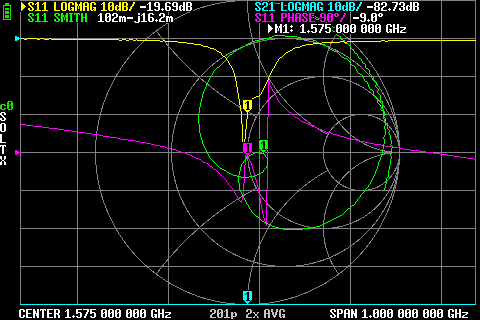
If you’ll look back at the simulated S11 you’ll see it’s pretty close! Exciting stuff.
GPS!!!
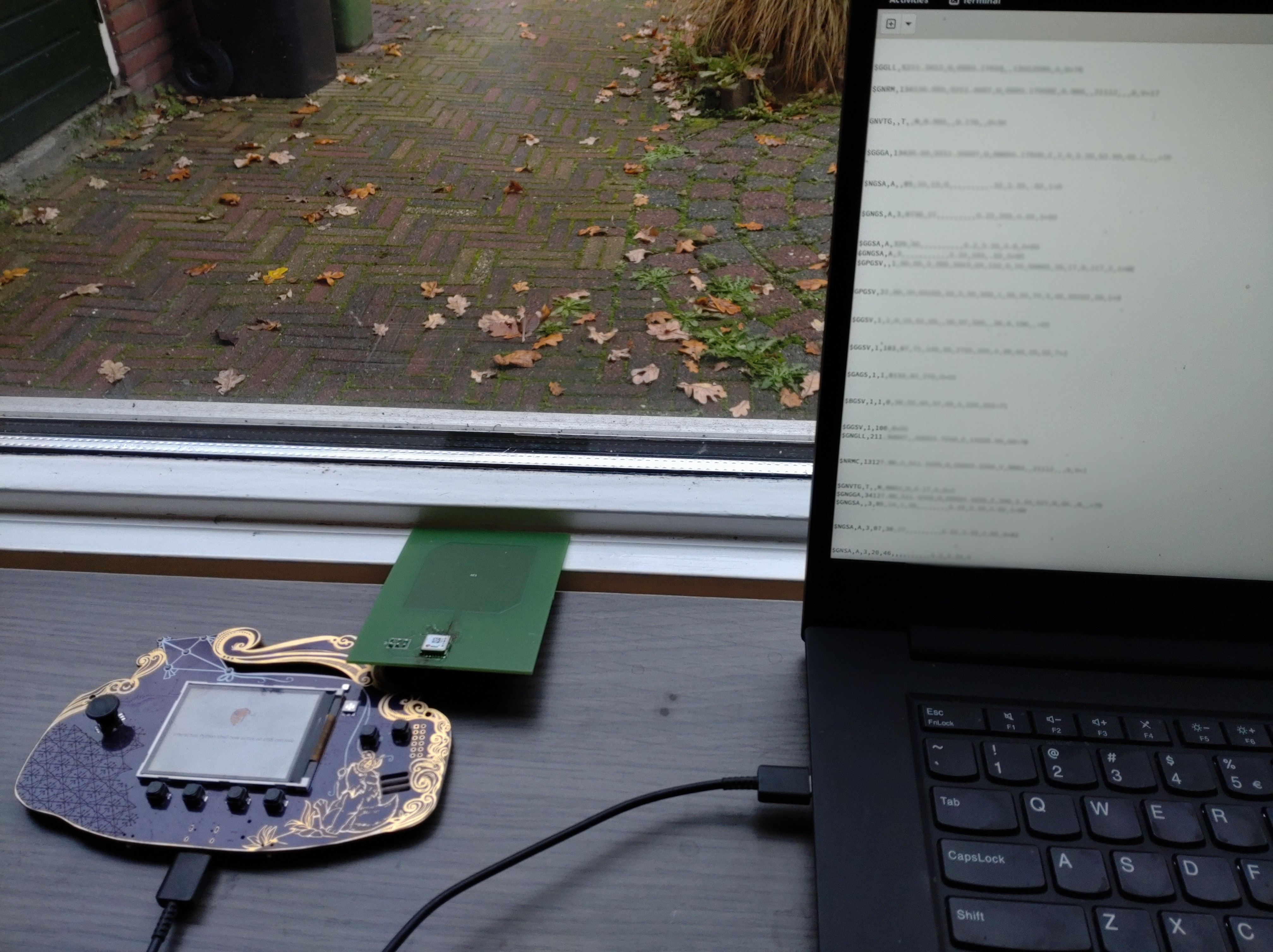
So of course the next step is to actually receive GPS signals with it. But how? I went for a two-pronged approach. I ordered an RTL-SDR, which I read can do GPS, and I ordered a PCB with my patch antenna and an u-blox MAX-M10S.
I never got to the SDR part, because the u-blox actually worked!!! It took a bit of fiddling to figure out how the I2C interface worked, but what you see in this picture is my GPS SAO PCB plugged into a MCH badge spewing NMEA messages to my laptop. I blurred the details, but it actually saw satelites and found my location!
All the stuff is on github although it’s more about the process than drawing a 45mm pad ;)